So you are working on a project that needs a custom circuit. You created a prototype on the perf board and it works fine. But what if you want multiple copies of the same circuit board? Making the same circuit 10 times and going through all the wiring and troubleshooting can be tiring and boring.
But, there is a solution! Building a professional Printed Circuit Board (PCB) is now fast and cost-effective. In this tutorial, I’ve outlined the steps to help you start designing and ordering your own PCBs and transforming your projects into polished, professional-looking products.
Requirements:
To start building a PCB one first needs the following things:
- Circuit Diagram: You should always design a rough schematic for your project.
- EDA Software: For designing the PCB, you’ll need Electronic Design Automation software. We’ll be using EasyEDA, an excellent free tool ideal for beginners to learn from.
Creating the Schematics:
Start by visiting EasyEDA and creating an account. As it’s an online service, the server stores all projects. After signing up:
Upon logging in, you’ll encounter a blank canvas. Positioned at the top and left side of the canvas are various menus and tools essential for designing the circuit.
- From the Top menu go to Files >> New >> Project.
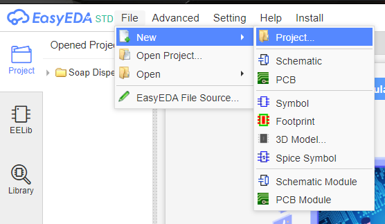
- A pop-up window will appear. Here, input the name of your project, then click on the “Save” button to proceed.

- Now, you’ll see a blank canvas where you’ll create the schematic. Begin by accessing the required components from the parts library.
- To access the components, click on “Library” from the left toolbar. This action will open a window where you can search for the required component.
- Choose the desired component from the list, then double-click to place it on the canvas.
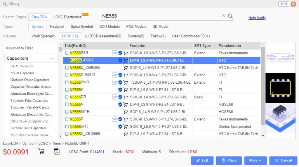
- After dropping the components onto the canvas, you can begin connecting them according to the rough schematic you created.
- To make the connection between two pins one can either use a wire or a netport.
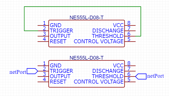
In the image above, you can observe how wires and net ports facilitate connections between two pins. You can access both from the wiring tools menu located at the bottom right corner.

While using the net ports, make sure that the ports connecting two pins should have the same label.
- Once all connections are made, Double-check to ensure that all connections align with your rough diagram.
- Now to design a PCB this schematic needs to be converted. To do that, click on “Design” on the top menu and select “Convert to PCB”.
- A new tab will open with a pop-up window asking for board dimensions. Here enter the preferred board size and shape.
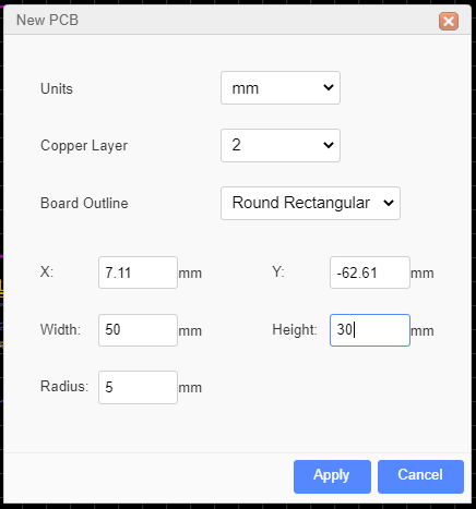
- On the new tab, you’ll find a board outline and component footprints. All you need to do now is to arrange the components on the board. Ensure that you maintain proper spacing, and place parts that connect together closer to each other.

- Referencing the schematic, connect the components accordingly. You can adjust the track width and clearance from the menu located on the right side of the interface.
- The ideal track width I prefer is 0.5mm but you can refer to the following chart to decide which width to use based on the current flow.

- While connecting tracks I avoid GND pins. I rather fill it with the copper plane. This helps with giving a good structure to the PCB and dissipates heat from components.
- To begin, finish routing the connections, then select the Copper Area tool from the PCB tools menu. Click on the four corners to cover the entire PCB. This action will create a GND plane.
With that being done, the PCB is ready. Now you just need to test the PCB recheck it and download the gerber files.
Checking Nets and DRC:
Now before converting the PCB into a gerber, it is important to check if all connections are made. Also, need to check the DRC (Design Rule Checking) to see if there are any problems in the routing. To do so:
- Select “Design Manager” from the left menu.

- Begin by clicking on the reload symbol next to “nets.” This process will unveil any missed connections and display errors if they exist. Clicking on the symbol will then highlight the pins lacking connections.
- Next, click on the reload button next to “DRC Errors.” This action will check for any design errors such as track clearance or hole diameters. If the system detects any errors, it will highlight them for your attention.
When all the design rules are error-free, you can make this into a Gerber file as explained below:
Converting into Gerber and Ordering PCBs:
After making the connections and routing the PCB, the next step is obtaining the Gerber files. These files are necessary for PCB manufacturers to print the board.
Talking about PCB manufacturers, PCBway is a PCB manufacturer from China that builds custom PCBs with a minimum order quantity of 5 PCs. They are also the sponsor of this tutorial.
The earlier designed board featured a NE555-based LED flasher circuit, used for demonstration purposes. I recently ordered PCBs for another project. But now let’s see how to generate Gerber and order PCBs.
- First, click on the “Fabrication” option from the top menu and select “PCB fabrication file(Gerber)”.
- You will get a popup asking if you want to check the DRC. If you haven’t done that already, I recommend doing it here otherwise, you can click on “Generate Gerber”.

- You will get a window as shown in the image above. Here click on “Generate Gerber” on the bottom right. A Zip file will be downloaded.
- Now head over to PCBway and create an account. Next, select “PCB instant quote” and click on “Quick-order PCB”.

- Click on “+Add Gerber file”, Navigate to the downloaded Zip file and open it. The file will then be uploaded to PCBway for an instant quote.
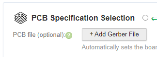
- Upon completion of the upload, you can choose the SolderMask colour according to your preference. Personally, I like Green or Blue, as they give a more professional look to the PCB.

- After selecting a preferred colour, select your country from the right menu and click on “Save to cart”.
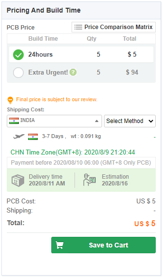
- Once you’ve added the PCB to your cart, you’ll have to wait for its review. If technicians detect any errors, they’ll notify you, enabling you to edit the files and re-upload them as necessary.
- Next, you’ll need to provide your name, address, and phone number. Once you’ve filled in this information, you can proceed to place your order and await the arrival of the PCBs at your doorstep.
Finally:
So I received the PCBs after 15 days and at first impression they were amazing. Below I have attached some images of the PCB design, 3D view, PCBs, etc.


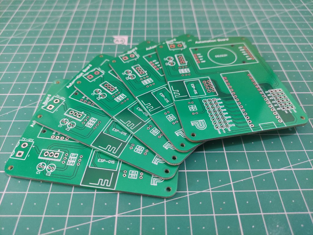

I will be sharing a detailed post about this project in future. Till then I hope you liked this tutorial and learnt how to design PCB.
If you have any questions, feel free to ask in the comment section. Also, I would like to share that we build custom projects and PCB designs, so if you are looking for our service feel free to contact us.

5 thoughts on “How to design a PCB”
Would it be possible for you to share the gerber design file you created? I am missing the connections. I have a few of the components like the ESP8266, but I can’t tell where a few of those connections occur.
Unfortunately, I can’t seem to find the Gerber files. But I can help you with the connections.
Contact me through email or WhatsApp and share what issues you are facing.
I need eda software download links
All links are provided in the article.